
PhD Thesis Final Defense to be held on January 30, 2020, at 14:00
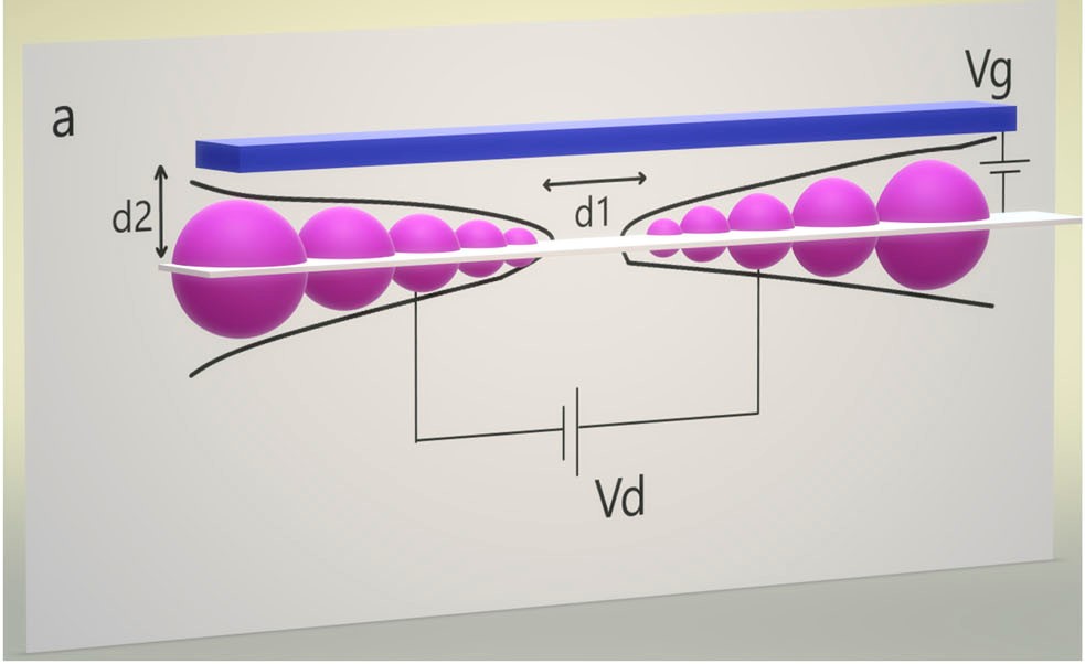
Photo Credit: Menelaos Tsagkarakis
The examination is open to anyone who wishes to attend (Room 2.1.19, Old ECE building).
Thesis Title: Tunneling currents inside nanoelectronic strain sensors and vacuum transistors
Abstract: Most applications of field emission have so far involved planar emitting surfaces and approximately 1-dimensional potentials. However, with the advent of nanotechnology and the fabrication of carbon nanotubes and emitting tips of nanometer radius of curvature the need has arisen for the description of such applications –where a multi dimensional electrostatic potential is involved by a numerical WKB theory of much greater accuracy than the traditional Fowler-Nordheim which is valid only for planar surfaces. This is the basic aim of this doctoral thesis. We have examined two such applications, the recently invented vacuum transistors with naonmetric emitters and collectors and the strain sensors with carbon nanotubes immersed in a dielectric medium. In both cases the sharp pointed emitting nanometric surface was represented by a collection of spheres. The advantage of such representation is that the Laplace equation could accurately be solved without the need of finite differences or elements. The spherical image potential was then added to the calculated electrostatic potential and the sum was used as the tunneling potential in multidimensional WKB approximation which was implemented numerically to calculate the transmission coefficient and finally the current.
In the case of strain sensors and due to the randomness of the immersion process the CNTs are at random angles and configurations between them, thus producing a 3-dimensional potential (3-D). We have then shown that the tunneling currents between a pair of CNTs depend critically on their relative angle and configuration. In particular, we have shown that the tunneling currents do not occur only along a CNT tip to CNT tip configuration but other more efficient paths exist which give a current higher by two orders of magnitude from what a simple 1D theory would give. On the other hand, the tunneling current between non-coplanar CNTs is negligible. We conclude that such phenomena cannot be analyzed by a simple 1-dimensional WKB theory and the percolation threshold necessary for conduction may be lower than the one such a theory would predict.
We have then calculated the electrical characteristics of a vacuum transistor withsharp, pointed emitter and collector with a radius of curvature R<20nm with the aim of revealing the advantages of such emitters. For such surfaces the traditional Fowler-Nordheim theory which pertains to a parallel plate configuration is not valid. We have used a 3-dimensional WKB theory capable of calculating the distribution of the current in space. We have shown that for values of emitter radius in the range of a few nanometers the current density is enclosed within a cone of angle of approximately 6°–16° thus minimizing current losses. The Id–Vd characteristics were calculated and found to exhibit a exponential behavior and a saturation region spanning currents from 10−14A to 10−6A by only 2 Volts change in gate voltage Vg, i.e. exhibiting an extraordinary transconductance.
Supervisor: John P. Xanthakis, Professor
PhD student: Menelaos Tsagkarakis